
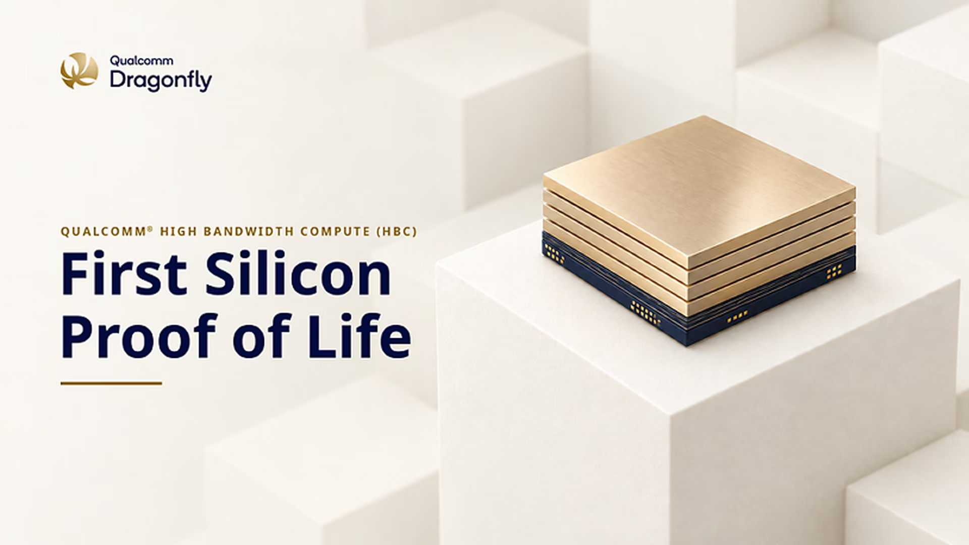
Scheduled to begin sampling during the initial six months of 2027, the forthcoming Dragonfly AI250 accelerator aims to redefine server-side machine learning performance. The unit boasts an effective memory throughput of 133TB/s per card, representing an eighteenfold increase compared to the company’s prior AI200 module. Designed for integration into the Dragonfly Rack server system, this hardware is engineered to assist cloud providers, hyperscale operators, and major corporations in expanding artificial intelligence processing while simultaneously curbing operational expenses and electrical demands.
This advance relies on High Bandwidth Compute (HBC) architecture, a mechanism created to eliminate the traditional latency encountered when transferring information between computational engines and storage during large language model execution. By positioning computing units adjacent to storage components, the configuration dramatically shortens the path data must travel, thereby elevating throughput and maximizing operational productivity per watt of electricity. Constructing this platform demanded close collaboration with semiconductor foundries and packaging firms to perfect wafer-to-wafer bonding, which physically attaches layers of DRAM over logic dies. Additionally, the architecture incorporates redundant memory space alongside dynamic remapping features to ensure uninterrupted performance around faulty storage cells.
Experimental validation was recently completed within Qualcomm’s San Diego facilities utilizing standardized automated diagnostic gear. Research teams evaluated both the complete memory read-and-write pathways along with in-memory computations using randomized datasets scaled to mimic enterprise-grade workloads. Following these successful evaluations, the semiconductor designer has finalized the silicon blueprint and dispatched the design to the factory for production—a milestone commonly designated as tape-out. Engineers have already initiated initial bring-up procedures on the synthesized logic substrate topped with direct-bonded DRAM layers.
While best recognized for powering mobile devices through its Snapdragon lineage, the enterprise expanded its server ecosystem by unveiling the Dragonfly product family in June. This current breakthrough builds upon more than a decade of internal research focused on integrating logic and memory layers in three dimensions. The chipmaker previously distributed hardware containing direct DRAM-to-logic bonds and helped establish the LPDDR standards ubiquitous in modern cellular phones. Though internal trials verified anticipated performance and energy savings, comparative metrics against rival processors remain modeled projections subject to variation based on final deployment conditions and active software workloads.













Leave a Reply